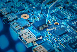
In our modern world, nearly every electronic device we rely on—from smartphones and laptops to medical equipment and electric vehicles—depends on a small but essential component known as a Printed Circuit Board (PCB). Often called the “backbone” of electronics, a PCB mechanically supports and electrically connects electronic components using conductive pathways etched from copper sheets laminated onto a non-conductive substrate.
Understanding what a PCB is and how it works is fundamental for anyone interested in electronics, whether you’re a student, hobbyist, engineer, or simply curious about technology. This educational guide will walk you through the basics, history, types, materials, manufacturing process, and future trends in PCB technology, drawing from established industry knowledge and standards.
The History of PCBs: From Early Innovations to Modern Essentials
The concept of printed circuits dates back to the early 20th century. In 1903, German inventor Albert Hanson described flat foil conductors laminated to an insulating board in multiple layers. Further experiments by Thomas Edison in 1904 involved chemical plating on linen paper, while patents in the 1910s and 1920s explored print-and-etch methods.
The true breakthrough came in 1936 when Austrian engineer Paul Eisler invented the modern PCB for a radio set. During World War II, the technology advanced rapidly: the U.S. military used it for proximity fuzes in artillery shells, and multi-layer designs appeared in German naval mines. Post-war, the U.S. declassified the technology in 1948, leading to commercial adoption in the 1950s for transistor radios and televisions.
Through-hole technology dominated initially, with components inserted into drilled holes and soldered. The 1960s introduced surface-mount technology (SMT), allowing components to be placed directly on the board’s surface. By the 1980s and 1990s, SMT and multi-layer boards became standard, enabling smaller, more powerful devices. High-Density Interconnect (HDI) technology emerged in the 1990s with microvias for even denser designs.
Today, the global PCB market exceeds $80 billion, projected to reach nearly $100 billion by 2029, driven by demand in consumer electronics, automotive, and telecommunications.
How Does a PCB Work?
At its core, a PCB replaces messy point-to-point wiring with organized, reliable conductive tracks. Here’s a simple breakdown:
- Substrate: The base material provides mechanical support and insulation.
- Copper Layers: Thin sheets of copper are laminated onto the substrate and etched to form traces (wires), pads (for component attachment), and planes (for power/ground distribution).
- Vias: Small plated holes that connect traces between layers.
- Solder Mask: A protective layer (usually green) that prevents shorts and corrosion.
- Silkscreen: Printed labels for component placement and identification.
Components like resistors, capacitors, and integrated circuits (ICs) are mounted on the board—either through holes (through-hole technology) or directly on the surface (SMT)—and soldered in place. This creates a complete circuit that controls electrical signals efficiently.
PCBs ensure signal integrity by managing factors like impedance, electromagnetic interference (EMI), and heat dissipation. In high-speed applications, precise trace widths and layer stacking maintain performance.
read more : The Role of Downloadable Social Media Videos in Daily Digital Life
Types of PCBs: From Simple to Advanced
PCBs come in various configurations to suit different needs:
1. Single-Sided PCBs
The simplest type, with copper traces on one side only. Ideal for basic, low-cost applications like calculators or LED lights.
2. Double-Sided PCBs
Copper on both sides, connected by vias. Common in more complex devices like power supplies or audio equipment.
3. Multi-Layer PCBs
Multiple layers (4 to 64+ in advanced cases) stacked and bonded together. Internal layers often serve as ground or power planes for better noise reduction and routing density. Used in smartphones, computers, and servers.
4. Flexible PCBs
Made from flexible materials like polyimide (Kapton). They bend or fold, perfect for wearables, cameras, and compact devices.
5. Rigid-Flex PCBs
A hybrid combining rigid sections for component mounting with flexible sections for interconnections. Common in aerospace, medical devices, and foldable electronics.
6. High-Density Interconnect (HDI) PCBs
Feature microvias (smaller than 150 μm), blind/buried vias, and finer traces for ultra-compact designs. Essential for modern smartphones, 5G devices, and AI hardware.
Other specialized types include metal-core PCBs (for heat dissipation in LEDs) and aluminum-backed boards for power electronics.
Materials Used in PCBs
Material selection balances cost, performance, durability, and environmental factors:
- Standard Substrate: FR-4 (fiberglass-reinforced epoxy) is the most common—affordable, flame-retardant, and suitable for temperatures up to 130–170°C.
- High-Performance: Rogers or Teflon-based for low-loss, high-frequency applications (e.g., RF/microwave).
- Flexible: Polyimide for bendable boards.
- Metal-Core: Aluminum or copper for thermal management.
- Eco-Friendly: Halogen-free and bio-based options are gaining traction for sustainability.
Copper thickness (typically 1–2 oz/ft²) affects current-carrying capacity. Surface finishes like ENIG (Electroless Nickel Immersion Gold) protect pads and improve solderability.
Industry standards from IPC (the global electronics association, formerly Institute for Printed Circuits) ensure material quality and reliability, such as IPC-4101 for laminates.
The PCB Manufacturing Process: Step by Step
Modern PCB production is highly automated:
- Design: Using software to create schematics and layouts.
- Artwork Preparation: Generating patterns for each layer.
- Lamination: Stacking and bonding substrates with copper foils.
- Drilling: Creating holes for vias and components.
- Etching: Removing unwanted copper to form traces.
- Plating: Depositing copper in vias and on surfaces.
- Solder Mask Application: Coating for protection.
- Silkscreen Printing: Adding labels.
- Surface Finishing and Testing: Electrical tests, AOI (Automated Optical Inspection), and X-ray for defects.
- Assembly: Mounting and soldering components (PCBA).
Advanced processes like laser drilling enable HDI features. Compliance with RoHS (Restriction of Hazardous Substances) ensures lead-free, environmentally safer production.
Why PCBs Matter: Applications and Importance
PCBs enable miniaturization, reliability, and mass production—key to today’s connected world. They’re in:
- Consumer devices (phones, TVs)
- Automotive (EV battery management, ADAS)
- Medical (implants, diagnostics)
- Aerospace and military
- IoT and 5G infrastructure
Without PCBs, modern electronics would be bulkier, less reliable, and far more expensive.
Current and Future Trends in PCB Technology (as of 2025)
As electronics evolve, so do PCBs:
- Miniaturization and HDI Growth: Finer features for AI servers and 6G.
- Flexible and Rigid-Flex Boom: For wearables and foldables.
- Sustainability: Recyclable materials, reduced waste, and green manufacturing.
- High-Frequency Materials: Supporting faster data rates.
- Automation and Industry 4.0: AI-driven design and inspection for higher yields.
- Embedded Components: Integrating passives into substrates for compactness.
The market is shifting toward eco-friendly, high-performance boards amid growing demand from EVs and AI.
Conclusion: The Foundation of Modern Electronics
A printed circuit board, or pcb board, is far more than a simple green plate—it’s a sophisticated platform that powers innovation across industries. From its wartime origins to today’s advanced HDI and flexible designs, the PCB has revolutionized how we build and interact with technology.
Whether you’re designing your first circuit or exploring electronics as a hobby, grasping PCB fundamentals opens doors to deeper understanding. For more in-depth resources, consult IPC standards or reliable educational sites. The future of PCBs promises even smarter, greener, and more capable boards—continuing to drive the electronics revolution forward.